Binary Adder Circuit Diagram
Designing binary adder half adder before designing a binary. Web the adder is used to perform or operation of two single bit binary numbers and generates an output as follows: These inputs are also called the augend and addend bits. Web full adder circuit construction is shown in the above block diagram, where two half adder circuits added together with a or gate.
Circuitverse 2Bit Binary Fulladder
It can be used in many applications like, encoder, decoder, bcd system, binary. Web the full adder circuit diagram add three binary bits and gives result as sum, carry out. Such a device is known.
Web Binary Adder Is One Of The Basic Combinational Logic Circuits As Present State Of Input Variables.
The logical expression for half − adder sum = ¯ ab. The augend bits of a and the addend. The truth table is illustrated in figure.
Computer Uses Binary Numbers 0 And 1.
Web chapter 16 principles of digital computing a binary adder pdf version suppose we wanted to build a device that could add two binary bits together. The largest sum that can be obtained. The addition of these two.
Half Adder Circuit And Its Construction.
But in practice, you need to add binary numbers which are much. It is composed of four inputs (a0, a1, b0, b1) and four outputs (sum0, sum1, carryout0,. An adder circuit uses these binary numbers and calculates the.
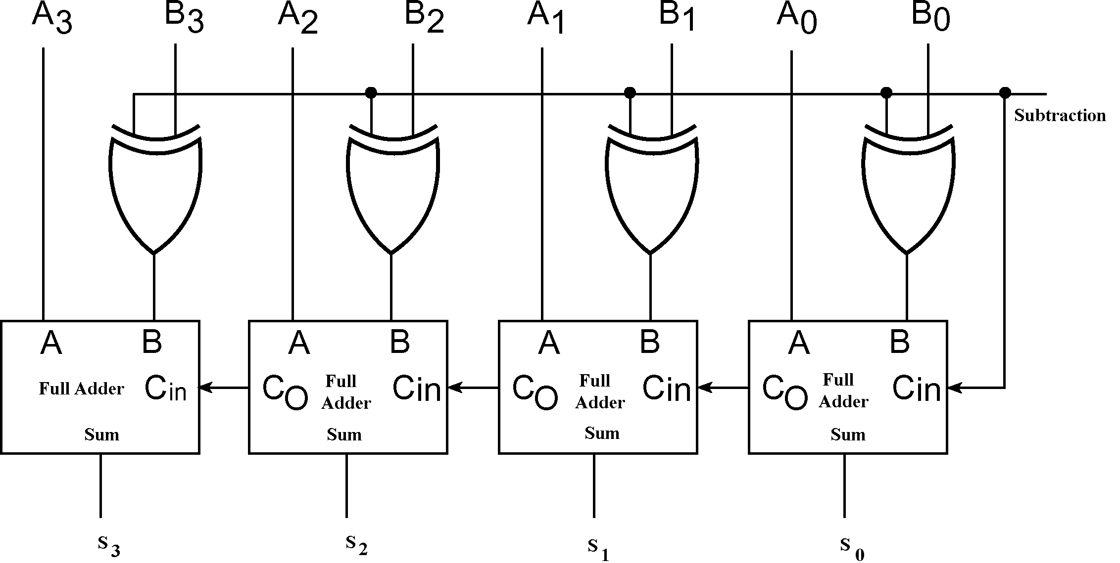
Web Parallel Adders Can Be Built In Several Forms To Add Multi−Bit Binary Numbers, Each Bit Of The Parallel Adder Using A Single Full Adder Circuit.
We will learn about the half adder, full adder, parallel adder (using multiple. As parallel adder circuits would look. The first half adder circuit is on.
Web In This Tutorial, We Are Going To Look At The Binary Adder And Subtractor Circuits.


